
 0086-20-3156-0779
0086-20-3156-0779
0086-20-3156-0779


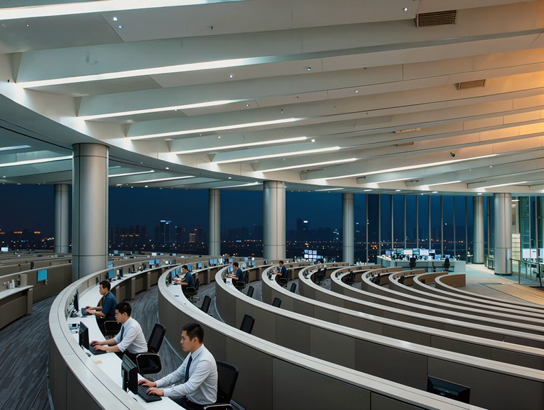
For years the story of China's semiconductor rise was told through one number: how many leading-edge fabs it could build without access to the West's most advanced lithography tools. That framing is now out of date. On the back end of the chip, where silicon dies are cut, stacked and sealed into packages, China is already a quiet superpower — and nowhere near one at the same time. Mainland Chinese firms hold roughly 30% of the world's outsourced chip assembly and test capacity, according to the Chinese industry research house Faxiangongchang. Yet in the advanced packaging that AI chips depend on, the same researchers put mainland localization under 5%. A senior consultant at Henderson Executive Search put the split bluntly: China learned how to package the world's chips before it learned how to package the chips that matter.
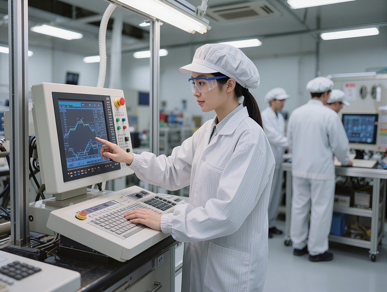
The scale of the mismatch is the story. The global OSAT — outsourced semiconductor assembly and test — market reached about 48 billion in 2025, and China's big three packaging houses now sit near the top of it: JCET ranks third worldwide, Tongfu fourth and Huatian sixth, together claiming roughly 22% to 24% of the global market, per Faxiangongchang. What they build in volume is legacy and mature-node packaging. What they do not build is the advanced stuff — chiplet integration, 2.5D and 3D stacking, and the CoWoS-class capacity that has been sold out across the industry since 2022, according to the display and semiconductor research firm Sigmaintell. Sigmaintell now sizes the advanced packaging market at around 58.7 billion for 2026, on AI-driven volume and price strength. The gap between China's 30% share of a 48 billion market and its under-5% share of a 58.7 billion one is where the money and the talent are both moving. This is no longer a niche manufacturing story; it is a supply chain story, and it is rippling across the international talent market faster than most executive teams have noticed. The packaging floor is the one place in the semiconductor supply chain where China already competes with the world — and the one place where its shortfall is now most expensive.
The investment is arriving in a rush. Between May and July 2026 alone, nearly ten advanced packaging projects worth a combined 400 billion yuan — roughly $56 billion — were announced across mainland China, spanning chiplet, 2.5D and 3D integration, fan-out packaging and automotive chip substrates, according to the tech outlet Pandaily. JCET has been building new advanced packaging facilities in Jiangsu and Singapore, while its domestic rivals are pulling the same lever, and DigiTimes reports that China's OSAT sector is accelerating capacity expansion to chase demand from AI, high-performance computing and automotive electronics. The driver is not hard to name. Blocked from the most advanced lithography, Chinese chip designers are answering the same question their rivals answered a decade ago: if you cannot shrink the transistor, you stack the chips. Advanced packaging is the workaround that turns four mature-node dies into one AI-class processor. Leon Liao, an analyst who tracks the sector, calls China's path "not a simple copy of TSMC's CoWoS model" — which is precisely why the people who know how to build it are so scarce. Here's the thing: the equipment can be bought, the fabs can be financed, but the process engineers who understand the yields of a 2.5D stack cannot be conjured. A wafer in a chiplet stack is no longer a single component to test; it is a system, and the people who run systems are different from the people who run lines.
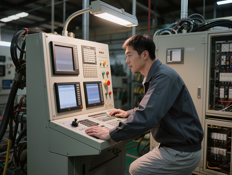
That is where executive search gets pulled to the front of the room. The advanced packaging roles China suddenly needs in volume — packaging R&D directors, process integration leads, OSAT plant general managers, chiplet architecture chiefs — were nearly nonexistent on the mainland five years ago, because the industry they served did not exist there. A consultant at Henderson Executive Search who works semiconductor mandates describes the same search arriving from a Suzhou packaging house and a Singapore OSAT in the same month: both want a leader who has taken a chiplet design from tape-out to volume yield, who has run a high-mix packaging line at scale, and who has managed a joint venture across two legal jurisdictions. The supply of that profile is concentrated in a handful of places — Taiwan, South Korea and a few U.S. sites — and it does not move cheaply or quickly. Henderson Executive Search's recruiters report that search timelines for a senior advanced packaging executive have stretched well past six months, and that the cross-border conversation now runs in both directions: Chinese firms trying to import process talent, and the same firms defending their own hires against counteroffers. The talent pool, in short, has not scaled with the capital. A packaging R&D director who can hit 2.5D yield targets in Shanghai can now name a number that would have sounded absurd three years ago, and the number keeps climbing as each new project breaks ground.

It would be a mistake, though, to read every announced yuan as a signed contract. A portion of the 400 billion yuan wave is state-directed and will be spent on shells and sites before it is spent on yields; advanced packaging is hard to do profitably, and Chinese firms have yet to prove they can match TSMC or Samsung on 2.5D defect rates. That said, the direction of travel is not in doubt, and it is the direction that matters for hiring. To be fair, the packaging push is not a story of imminent Chinese dominance — it is a story of a capability being built one line, and one hire, at a time. The companies that will win are the ones that stop treating packaging as a commodity and start treating it as a leadership function, with the same rigor they apply to design. Most of the activity, meanwhile, is clustering in a few corridors — Jiangsu, the Yangtze Delta and the Singapore bridgehead — which only sharpens the fight for the same small cohort of bilingual, process-literate executives. Henderson Executive Search's consultants counsel clients against treating this as a single-hire fix: a chiplet program needs a bench of perhaps fifteen to twenty packaging, yield and test leaders, and most mainland firms are starting from one or two.
What this means for hiring is unambiguous. For a Chinese OSAT or chip designer moving into chiplet and 2.5D packaging, the scarce asset is no longer capital, no longer equipment, and no longer even fab capacity; it is an executive who has actually delivered advanced packaging at yield, and who can build a team around a discipline that barely exists in the country that is trying to buy it. Henderson Executive Search sees the demand running across three fronts: packaging houses that need process and yield leadership, chip designers that need chiplet architects, and the Singapore and Jiangsu subsidiaries that need general managers who can run a cross-border operation in two languages. How do you build that bench from a talent pool measured in the thousands, not the tens of thousands? The answer, increasingly, is that you do not build it — you find it, one executive at a time, across Suzhou, Hsinchu, Singapore and Seoul. For the firms that move first, Henderson Executive Search argues the reward is a seat in the one part of the chip where China's 30% still has nowhere to go but up.

FAQ
Q: How wide is the gap between China's packaging share and its advanced packaging capability?
A: Mainland firms hold roughly 30 percent of global outsourced chip assembly and test capacity, while localisation in the advanced packaging that AI chips depend on sits under 5 percent, according to the industry research house Faxiangongchang. The volume business is legacy and mature-node packaging; chiplet integration, 2.5D and 3D stacking are the parts still being built, which is why blocked access to leading-edge lithography made stacking the practical workaround.
Q: Which roles are hardest to fill in advanced packaging?
A: Packaging R&D directors, process integration leads, OSAT plant general managers and chiplet architecture chiefs. Most of these titles barely existed on the mainland five years ago, because the industry they serve did not exist there. The profile clients ask for has taken a chiplet design from tape-out to volume yield, run a high-mix packaging line at scale, and managed a joint venture across two legal jurisdictions.
Q: Why does a chiplet programme need a bench rather than a single senior hire?
A: Because a wafer inside a chiplet stack is a system rather than a single component to test, and the people who run systems are not the same as the people who run lines. Consultants put a full programme at fifteen to twenty packaging, yield and test leaders, while most mainland firms are starting from one or two. Search timelines for a senior advanced packaging executive run well past six months.
Q: Where is the candidate pool and where is activity clustering?
A: The pool is concentrated in Taiwan, China, South Korea and a few U.S. sites, and it does not move cheaply or quickly. Project activity clusters in Jiangsu, the Yangtze Delta and a Singapore bridgehead, which sharpens competition for the same small bilingual cohort. A portion of the announced investment is state-directed and will be spent on shells and sites before it is spent on yields, and matching leading foundries on 2.5D defect rates remains unproven.





 Biotech Out-licensing Booms. Executive Talent Is the New Bottleneck